SiC Processing Dust Collection. Shandong Tianyue Advanced Technology Co., Ltd. (SICC) ranks among the global top three silicon carbide substrate manufacturers. Therefore, when SICC built a new processing workshop in Jinan, dust purification became a critical priority. Specifically, the project addressed airborne contamination across slicing, grinding, polishing, and cleaning operations. Moreover, SiC dust poses unique challenges due to its extreme hardness and ultra-fine particle size.
Silicon carbide substrate manufacturing generates significant airborne particulates. Consequently, these particles threaten both product yield and worker health. Furthermore, SiC dust reaches Mohs hardness 9.5, which damages precision equipment surfaces. However, standard dust collectors cannot effectively capture sub-micron SiC particles. Therefore, a specialized SiC wafer processing dust collection system was essential.
Keywords: SiC wafer processing dust collection, silicon carbide dust purification, semiconductor workshop dust extraction, ultra-fine dust filtration system, SiC substrate manufacturing air filtration
Silicon carbide substrate production follows a rigorous process chain. Specifically, the workflow includes SiC powder synthesis, crystal growth via PVT method, wire slicing, lapping, CMP polishing, and final cleaning. Meanwhile, each processing stage generates distinct dust profiles.
SiC processing dust presents three critical challenges. First, particle size distribution ranges from 0.1 to 10 micrometers. Moreover, the 0.5 to 1 micrometer fraction dominates the output. Consequently, conventional filters with micron-level ratings cannot achieve sufficient capture rates.
Second, SiC particles carry extreme hardness. Specifically, at Mohs 9.5, silicon carbide ranks just below diamond. Therefore, airborne SiC dust abrades precision equipment surfaces, guide rails, and optical components. Furthermore, this abrasion degrades wafer processing accuracy over time.
Third, SiC processing generates mixed pollutants. Wire cutting produces oil-laden fumes alongside fine dust. Grinding and polishing create slurry-based wet particulates. Meanwhile, crystal growth furnaces release carbon particles and silicon oxide microspheres. Thus, a single-stage filter cannot address all contaminant types effectively.
Semiconductor manufacturing imposes strict air quality requirements. Specifically, particulate contamination directly reduces wafer yield. Moreover, even microscopic dust landing on a substrate surface causes circuit defects in downstream epitaxy and device fabrication. Therefore, the dust collection system must achieve filtration efficiency above 99.97% for particles at 0.3 micrometers and above.
In addition, China's electronic industry standard GB 39731-2020 mandates specific emission limits for semiconductor facilities. Furthermore, GB 16297-1996 sets comprehensive air pollutant discharge standards. Consequently, the purification system must satisfy both occupational health and environmental compliance simultaneously.
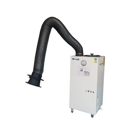
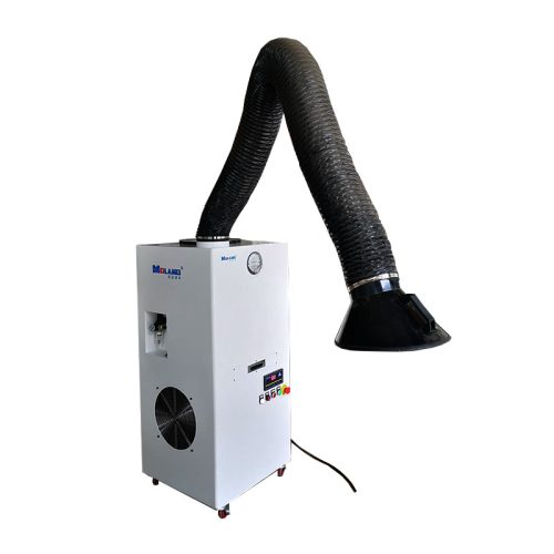
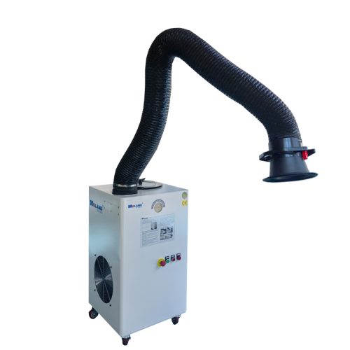
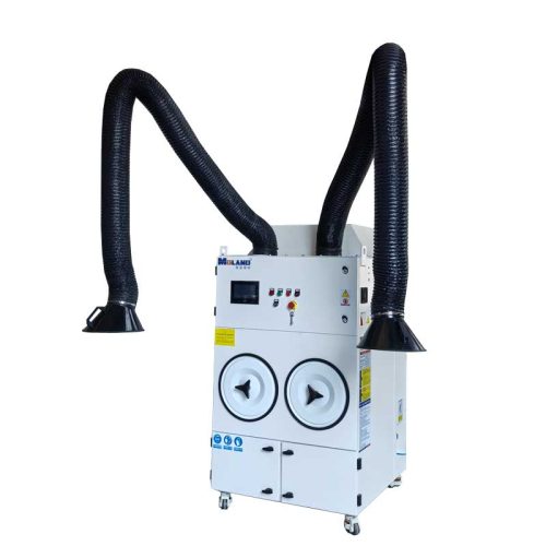
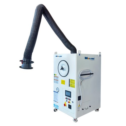
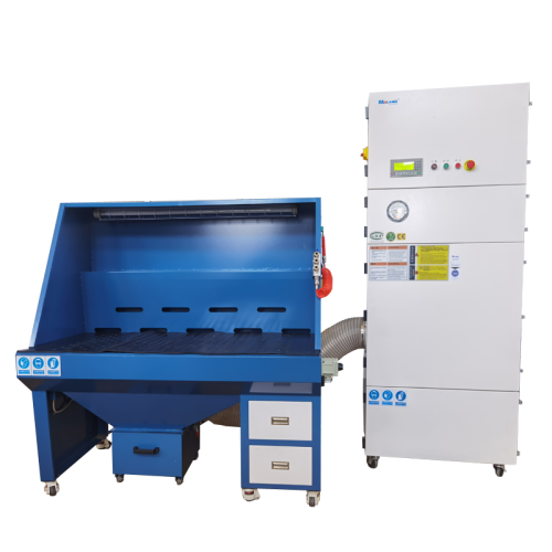
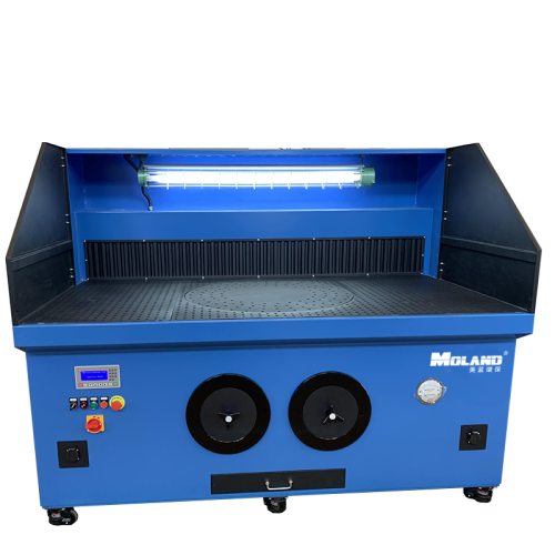
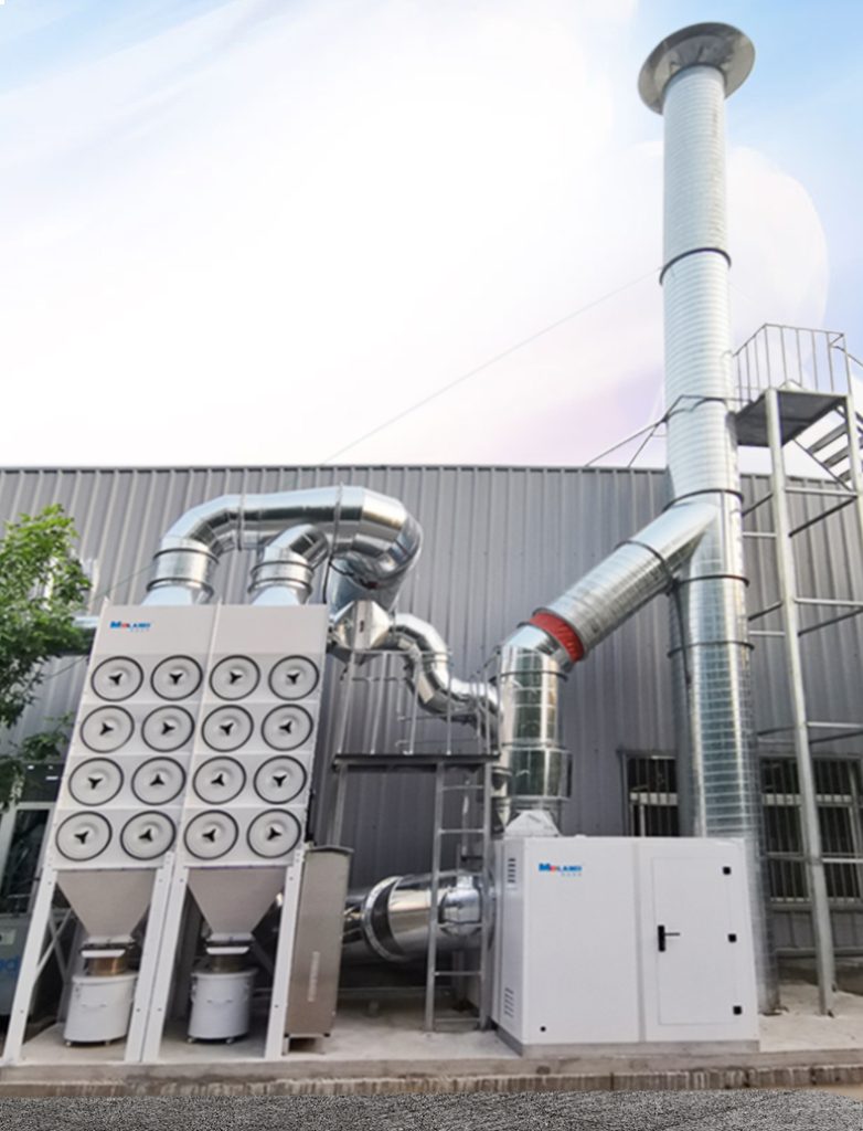
The SICC new workshop required a centralized high vacuum dust collection system. Therefore, Meilan designed a multi-point extraction network covering all dust-generating processes. Specifically, the system captures contaminants at each source point through dedicated suction hoods and enclosed process chambers.
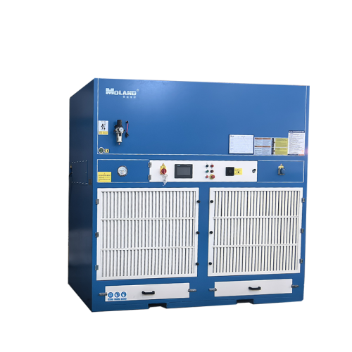
The centralized architecture offers several advantages. First, a single high-power host unit replaces multiple standalone collectors, therefore reducing equipment footprint. Second, consolidated filtration simplifies maintenance and filter replacement. Furthermore, the system enables organized emission through a dedicated stack. As a result, compliance monitoring becomes straightforward.
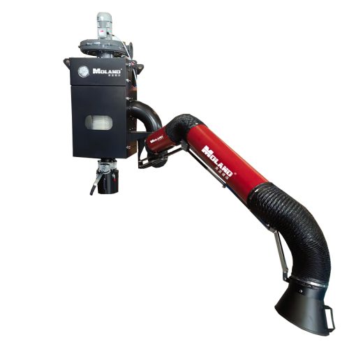
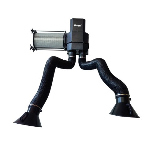
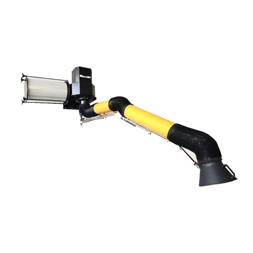
Effective SiC dust control begins at the source. Therefore, each processing station features purpose-built capture mechanisms:
Consequently, source capture prevents contaminants from entering the workshop atmosphere. Moreover, this approach reduces the load on central air purification systems significantly.
SiC dust demands careful ductwork engineering. Specifically, pipeline velocity must stay between 10 and 18 meters per second. Below 10 m/s, ultra-fine particles deposit on duct walls. Conversely, above 18 m/s, energy consumption rises sharply while noise levels increase. Therefore, Meilan calculated optimal duct diameters based on airflow requirements at each extraction point.
Furthermore, the duct layout minimizes bends and branch junctions. Meanwhile, smooth interior surfaces reduce friction losses. Consequently, the system maintains consistent suction across all collection points without excessive energy waste.
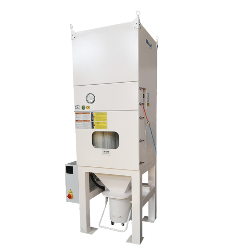
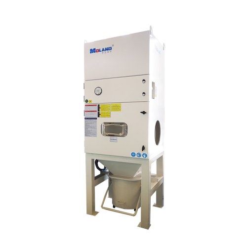
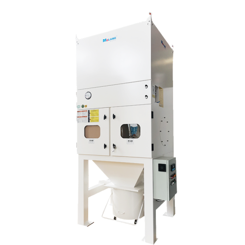
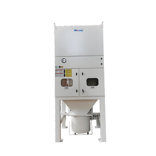
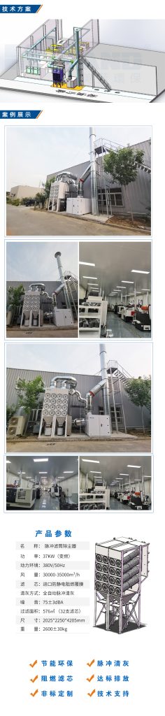
The filtration system employs a three-stage design. Specifically, each stage targets different particle size ranges and contaminant types:
Stage 1 — Pre-filtration (G4 grade): Synthetic fiber media captures particles above 5 micrometers. Therefore, large SiC debris, grinding swarf, and cutting residues are intercepted early. Moreover, this stage protects downstream filters from premature clogging. Consequently, the overall system lifespan extends significantly.
Stage 2 — Mid-stage filtration (F7-F8 grade): Fiberglass media captures particles between 1 and 5 micrometers. Specifically, fiberglass does not rely on electrostatic adhesion. Therefore, filtration efficiency remains stable under SiC processing conditions. Meanwhile, electrostatic-based media such as meltblown PP suffer rapid efficiency decay within 3 to 6 months in SiC environments. As a result, fiberglass is the mandatory choice for mid-stage filtration in semiconductor dust collection.
Stage 3 — High-efficiency filtration (H13 grade): PTFE membrane filter cartridges achieve 99.97% efficiency for particles at 0.3 micrometers and above. Specifically, PTFE employs surface filtration rather than depth filtration. Therefore, captured dust stays on the membrane surface for easy pulse-jet cleaning. Furthermore, PTFE membranes maintain stable performance for 3 to 5 years. Conversely, nano-coated membranes degrade to 98% efficiency within 1.5 to 3 years.
PTFE membrane technology provides critical benefits for SiC dust applications:
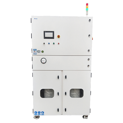
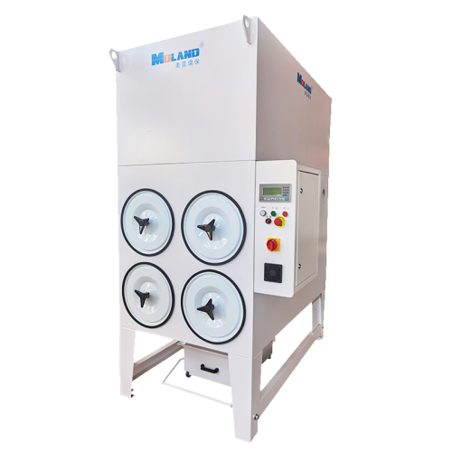
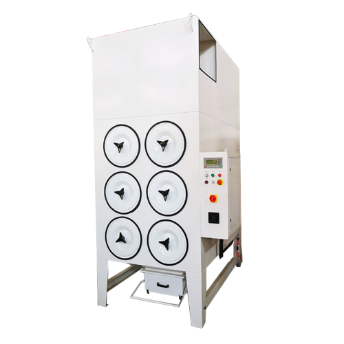
Meanwhile, the system incorporates automatic pulse-jet cleaning. Specifically, compressed air pulses reverse-flow through the filter cartridges at timed intervals. As a result, accumulated dust falls into the collection bin, restoring filter permeability without manual intervention.
SiC wafer processing generates more than just particulate dust. Specifically, wafer cleaning involves hydrofluoric acid, sulfuric acid, nitric acid, and hydrochloric acid. Therefore, acid fumes require dedicated scrubbing towers. Meanwhile, alkaline cleaning with ammonia solutions produces alkaline vapor. Consequently, the SICC project integrates both acid and alkali scrubbers alongside the dust collection system.
The acid scrubber uses sodium hydroxide spray to neutralize acidic gases. Conversely, the alkali scrubber employs sulfuric acid spray for ammonia absorption. Furthermore, both scrubbers connect to dedicated 15-meter emission stacks. Therefore, treated exhaust meets GB 16297-1996 discharge standards.
Seed crystal processing and wafer bonding generate organic solvent vapors. Moreover, wire cutting oil produces oily fumes during slicing operations. Therefore, the system includes specialized VOC treatment modules.
For oily fume control, an electrostatic oil mist eliminator captures and drains cutting oil residue. Meanwhile, a water wash plus activated carbon adsorption system treats organic vapors from bonding and cleaning processes. Specifically, the activated carbon unit achieves VOC removal rates above 90%. Consequently, emissions comply with DB37/2801.7-2019 standards for volatile organic compounds.
The SICC project designed all emission points for regulatory compliance. Specifically, exhaust stacks include reserved detection ports at standard heights. Moreover, permanent monitoring platforms with access ladders enable routine inspection. Therefore, environmental authorities can verify compliance without disrupting production.
Key compliance targets include:
表格
| Pollutant | Standard | Limit |
|---|---|---|
| Particulate matter | GB 16297-1996 Table 2 | Organized emission compliant |
| Sulfuric acid mist | GB 16297-1996 | Concentration ≤ 45 mg/m³ |
| Hydrogen chloride | GB 16297-1996 | Emission rate ≤ 0.75 kg/h |
| Hydrogen fluoride | GB 16297-1996 | Emission rate ≤ 0.05 kg/h |
| VOCs | DB37/2801.7-2019 | Concentration ≤ 60 mg/m³ |
| Ammonia | GB 14554-93 | Emission rate ≤ 4.9 kg/h |
Furthermore, workshop boundary concentrations meet unorganized emission limits. Consequently, the facility satisfies both occupational health and environmental protection requirements.
After system commissioning, workshop particulate concentration dropped significantly. Specifically, the high vacuum extraction network captures over 95% of generated dust at source. Moreover, PTFE membrane filtration ensures that recirculated air meets semiconductor cleanroom standards. Therefore, workers experience reduced exposure to respirable SiC particles.
In addition, improved air quality directly benefits product yield. Specifically, fewer airborne particles mean less contamination on wafer surfaces during processing. Consequently, the dust purification system pays for itself through yield improvement.
表格
| Parameter | Specification |
|---|---|
| Project location | Jinan Huaiyin District, Shandong |
| Client | Shandong Tianyue Advanced Technology Co., Ltd. (SICC) |
| Industry | SiC semiconductor substrate manufacturing |
| Dust type | SiC ultra-fine dust (Mohs 9.5), oil mist, acid/alkali fumes, VOCs |
| Particle size range | 0.1–10 μm (dominant fraction: 0.5–1 μm) |
| Collection method | Centralized high vacuum source capture |
| Filtration stages | 3-stage: G4 pre-filter → F7-F8 fiberglass → H13 PTFE membrane |
| Final filtration efficiency | ≥99.97% @ 0.3 μm |
| Auxiliary treatment | Acid/alkali scrubbers, electrostatic oil mist eliminator, activated carbon adsorption |
| Emission compliance | GB 16297-1996, GB 39731-2020, DB37/2801.7-2019, GB 14554-93 |
| Emission stack height | ≥15 meters with detection platform |
SiC dust destroys inferior filter media rapidly. Specifically, electrostatic meltblown PP cartridges lose efficiency within months. Therefore, fiberglass mid-stage filters and PTFE membrane final-stage cartridges are non-negotiable for semiconductor applications.
Waiting for dust to enter the workshop atmosphere before collecting it is ineffective. Instead, extraction at the generation point prevents contamination spread. Moreover, source capture reduces the total air volume requirement. Consequently, equipment size and energy consumption decrease.
SiC processing generates dust, oil mist, acid fumes, and organic vapors simultaneously. Therefore, a dust-only system leaves significant pollution unaddressed. However, an integrated solution covering all pollutant types ensures full compliance and protects worker health comprehensively.
Even the best filter cannot compensate for poor ductwork. Specifically, undersized ducts cause inadequate suction at source points. Meanwhile, excessive bends increase pressure drop and energy waste. Therefore, precise duct sizing and optimized routing are fundamental to system success.
Ready to solve SiC dust challenges in your semiconductor workshop? Contact Meilan for a customized ultra-fine dust filtration system — why risk product yield and worker health when precision engineering can deliver guaranteed compliance?